

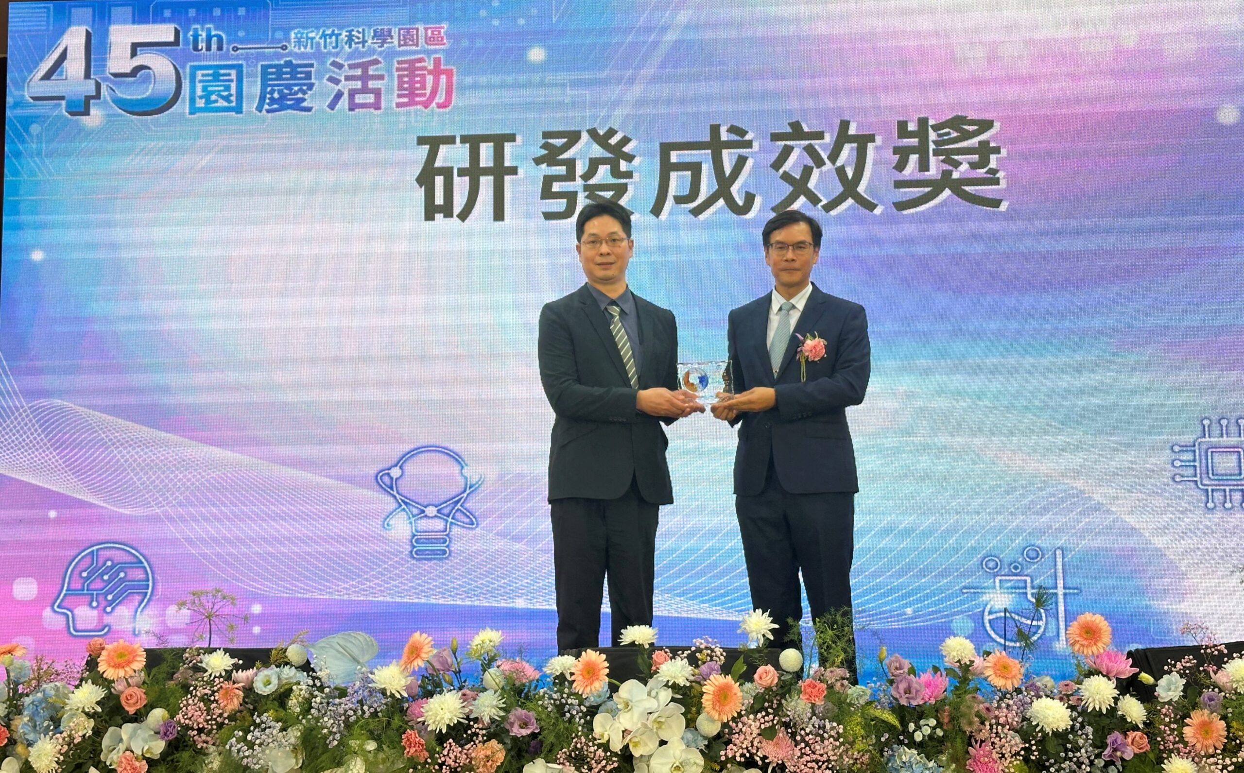
GlobalWafers has long positioned technological innovation and the deepening of research and development as the core of its corporate strategy. The company continues to invest in key materials and process technologies, while strengthening its intellectual property portfolio and talent development initiatives. Leveraging years of accumulated R&D achievements and innovation capabilities, GlobalWafers was awarded the “2025 Science Park R&D Accomplishment Award” by the Hsinchu Science Park, becoming the only company to receive this honor this year. In recent years, the company has further increased its R&D investment, focusing on advanced materials and technologies for third-generation semiconductors, including silicon carbide (SiC) and gallium nitride (GaN). This recognition not only affirms GlobalWafers’ R&D accomplishments in advanced materials, but also underscores its continued commitment to sustained R&D investment and industrial advancement.
GlobalWafers continues to invest in the development of materials and process technologies related to third-generation semiconductors, strengthening the process capabilities and supply stability of its SiC and GaN products to meet the growing demand for advanced materials in high-power and high-efficiency applications. Through the in-house development and continuous optimization of critical process technologies, the company has enhanced the process maturity and mass production capability of its SiC products, while gradually expanding its product portfolio in line with market demand. In the GaN segment, GlobalWafers has established product lines with scalable supply capability and continues to work closely with customers to advance product qualification and adoption. These products have received positive market feedback for their performance and quality. Overall, through steady R&D investment and process optimization, GlobalWafers continues to strengthen its key role in the global semiconductor supply chain and supports the ongoing advancement of the industry.
In recent years, GlobalWafers has continued to build a solid portfolio of research and development achievements at its Hsinchu and Zhunan sites, securing multiple patent positions in key process and materials technologies. With a strong focus on third-generation semiconductor–related technologies, this patent portfolio has helped establish a comprehensive and robust technological barrier. GlobalWafers has implemented the Taiwan Intellectual Property Management System (TIPS) for 13 consecutive years and has passed AA-level certification five times. The TIPS framework enhances systematic management of intellectual property acquisition, protection, and utilization, while enabling effective translation of R&D outcomes into patent portfolios or trade secret protection, thereby strengthening corporate competitiveness. The adoption and continuous optimization of the TIPS system played a critical role in demonstrating the company’s R&D capabilities and contributed positively to external recognition through this R&D Accomplishment Award.
GlobalWafers places strong emphasis on the cultivation and development of R&D talent. Internally, the company continues to expand its R&D teams at key research sites and actively recruits senior professionals to deepen its expertise in advanced materials and process technologies. Externally, GlobalWafers actively participates in various government-sponsored programs and industry–academia collaborations, promoting supply chain development and talent pipeline integration, and demonstrating tangible results in bridging academia and industry and fostering semiconductor talent.
Looking ahead, GlobalWafers will continue to place R&D at the center of its strategy, focusing on the advancement of high-performance and energy-efficient process technologies to support a wide range of applications, including electric vehicles, 5G, and AI. Through ongoing patent deployment and industry–academia collaboration, the company will further strengthen its technology accumulation and innovation momentum. By leveraging its R&D capabilities, GlobalWafers will continue to steadily advance the development of advanced materials and process technologies, helping customers enhance product performance and supply stability, while serving as a key and reliable partner in the global semiconductor value chain.