

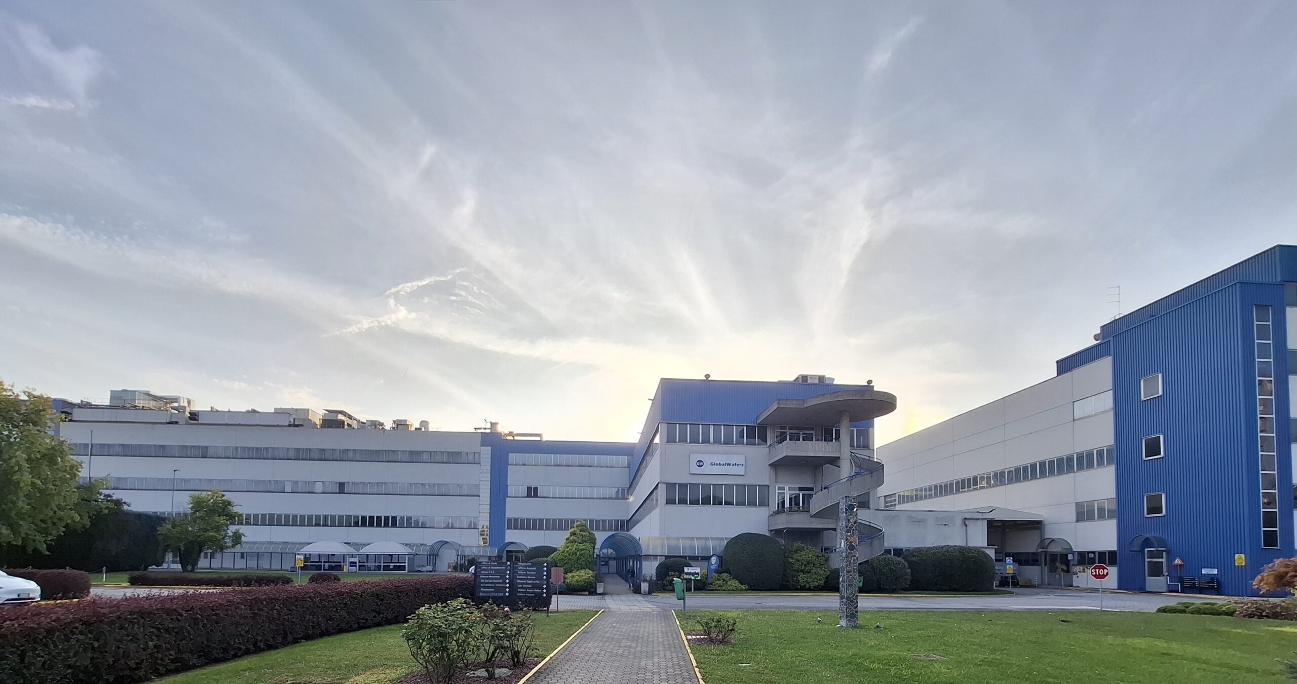
GlobalWafers Co., Ltd. officially inaugurated FAB300, its new 300mm semiconductor wafer manufacturing facility at MEMC Electronic Materials S.p.A. in Novara, Italy. The company positions FAB300 as one of Europe’s most advanced, fully integrated 300mm silicon wafer fabs.
The opening ceremony welcomed Hon. Adolfo Urso, Minister of Enterprises and Made in Italy; Sen. Gaetano Nastri, Italian Senate; Hon. Isabella Tovaglieri, Member of the European Parliament; Vincent Y.C. Tsai, Representative of the Taipei Representative Office in Italy; Alessandro Canelli, Novara Mayor; representatives of the Piedmont Region, together with distinguished guests; as well as hundreds of customers, suppliers, and partners who joined GlobalWafers in celebrating this historic milestone for European semiconductors.
Chairperson Doris Hsu stated: “FAB300 is not simply a manufacturing plant, it stands as a symbol of innovation, sustainability, and shared growth. It reflects the excellence, resilience, and outstanding execution of our Italian team, who have earned recognition across the European landscape. For GlobalWafers, customers, technical expertise and people have always been at the core of the company’s growth. FAB300 enables the company to work even more closely with customers to co-develop cutting-edge technologies, support their long-term growth strategies, and further advance Europe’s semiconductor ecosystem.”
In February 2022, GlobalWafers announced the expansion of its historic Novara site, which has produced silicon wafers since 1976, by adding a state-of-the-art 300mm fabrication module. This €450 million investment represents a strategic commitment to strengthening Europe’s semiconductor ecosystem.
As part of Europe’s coordinated industrial strategy to build technological sovereignty, FAB300 has been supported by €103 million in R&D funding through the second Important Project of Common European Interest on Microelectronics and Communication Technologies (IPCEI-ME/CT). This support, delivered through collaboration between the Italian Government and the European Union, recognizes the critical role FAB300 plays in advancing Europe’s semiconductor capabilities and building long-term resilience in the global supply chain.
Italian Senate, Sen. Gaetano Nastri stated: “The inauguration of FAB300 represents a fundamental step for Italy and for Europe: investing in the semiconductor supply chain means investing in the future, in technological sovereignty, and in qualified employment for our young people.”
Member of the European Parliament, Hon. Isabella Tovaglieri stated: “FAB300 represents a decisive step toward Europe’s technological independence, strengthening Italy’s role as a driving force for innovation and competitiveness. Investments like this are essential to building a stronger, more sustainable industrial future capable of creating opportunities for the next generations.”
The project has been developed in partnership with key European microelectronic device manufacturers, ensuring that production capabilities align with customer requirements and Europe’s strategic technology priorities.
“GWC has already demonstrated strong manufacturing capabilities across all silicon diameters, and we have no doubt that this new fab will become a success story. STMicroelectronics highly values GWC’s strategic decision to invest in Novara, close to our advanced manufacturing sites, bringing us sustainable supply robustness” said Chouaib Rokbi, Executive Vice President, Digital Transformation, Information Technology and Global Procurement of STMicroelectronics.
While the geopolitical context and economic headwinds have created new challenges for European competitiveness, GlobalWafers has remained steadfast in its commitment to Novara and to Europe. The successful completion of FAB300, delivering advanced manufacturing capability and creating up to 150 highly skilled jobs, demonstrates both the strength of the company’s long-term vision and the exceptional capabilities of the Italian workforce.
Novara Mayor, Alessandro Canelli stated: “The opening of FAB300 marks an event of extraordinary importance for our territory: an investment that creates qualified jobs, enhances local expertise, and reinforces Novara’s industrial vocation. Innovation generates employment when it is based on a shared vision among business, institutions, and community — and today we have tangible proof of that.”
In synergy with its Merano crystal growth operations, GlobalWafers offers one of Europe’s rare fully integrated 300 mm silicon wafer value chains, from crystal to finished wafer.
Once fully ramped, FAB300 will manufacture 300mm polished and epitaxial wafers using state-of-the-art, fully automated technology. These wafers will support advanced logic, memory, power, and MEMS/sensor application
The facility will operate under the RE100 standard, ensuring 100% renewable energy supply 100 %, significant water recycling (targeting ~50 %), and green manufacturing practices and reaffirming GlobalWafers’ global ESG commitments.
President of MEMC Electronic Materials S.p.A., Marco Sciamanna stated: “FAB300 is the result of vision, competence, and consistency — the key elements that made this achievement possible. With the strong support of our customers, institutions, and our outstanding Italian team, we are building not only the most advanced semiconductor facility in Europe, but also a model of determination and sustainable growth for the future.”
The close collaboration between the Merano and Novara sites creates a fully localized and efficient production network in Italy, enhancing flexibility, sustainability, and technological strength while reinforcing Europe’s semiconductor ecosystem.
Minister of Enterprises and Made in Italy, Hon. Adolfo Urso stated: “The inauguration of FAB300 confirms Italy’s leadership in the semiconductor sector and its commitment, together with Europe, to building a more autonomous and competitive supply chain. Only by uniting industry, education, and research can we strengthen our technological sovereignty and successfully face the challenges of the future.”
The success of FAB300 extends beyond GlobalWafers. Hundreds of best-in-class suppliers, from equipment manufacturers to engineering firms, have contributed advanced technology, systems, and expertise to the project. This collaborative approach strengthens the entire Piedmont region’s position in the global semiconductor value chain. GlobalWafers continues its long-standing collaborations with leading universities and research centers, fostering the continuous growth of Italy’s semiconductor ecosystem. These partnerships ensure knowledge transfer, talent development, and innovation that will benefit the region for decades to come.
FAB300’s inauguration follows the successful opening of GlobalWafers America (GWA) in Sherman, Texas, on May 15, 2025. Together, these facilities represent GlobalWafers’ commitment to geographic diversification and strategic partnerships with customers and governments worldwide.
300mm silicon wafers are the essential foundation for manufacturing leading-edge, mature-node, and memory chips. Silicon from GlobalWafers’ wafers is found in virtually every device that powers modern life, from home appliances, automobiles, and infrastructure to smartphones, computers, and artificial intelligence applications.
As Chairperson Hsu concluded: “Novara stands at the heart of GlobalWafers’ vision for semiconductor innovation in Europe. FAB300 strengthens Europe’s role in the global semiconductor value chain and enables the technologies that will define our future. Complemented by advanced manufacturing hubs across Asia, Europe, and the United States, GlobalWafers delivers a reliable, globally coordinated, and regionally anchored one-stop solution for 300mm wafers—from crystal growth to epitaxy wafers—ensuring consistency, efficiency, and long-term supply resilience. This is not just about manufacturing—it’s about partnership, resilience, and shaping a globally synchronized yet regionally empowered semiconductor supply network.”