
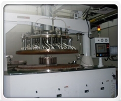
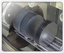
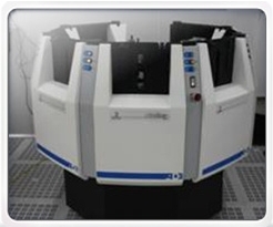
Slicing
Slice ingot to pieces of as-cut wafers
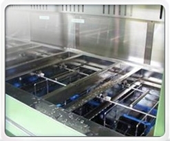
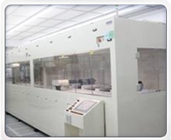
Wash out glue,slury and dirt on wafer surface after slicing
Fine grind edge of wafer to remove edge mechanical stress
Enhance wafer flatness
Wash out slury,metal dirt on wafer surface after lapping
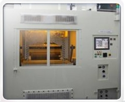
Remove surface damage caused by lapping process
Remove thermal donor cause by oxygen clusters
Make good extrinsic gettering to trap metal on the back side of during thermal process at epi house/foundry
Prevent substrate dopant going from backside of wafer,which benefit resistivity uniformity at front side
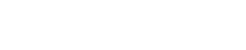
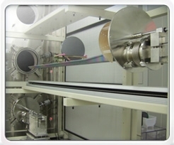
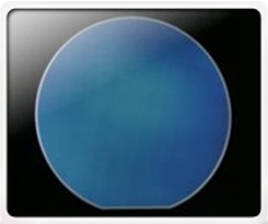
Make mirror-like surface ready for epi or device process
Remove slurry and reduce metal/particle level on wafers surface
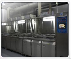
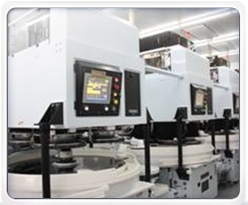
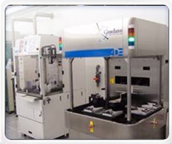
Inspect wafer geometry by automatic sorter
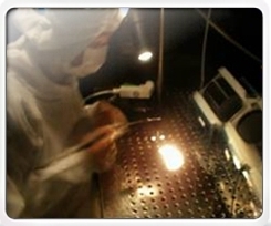
Inspect wafer appearance by naked-eye and auxiliary light source
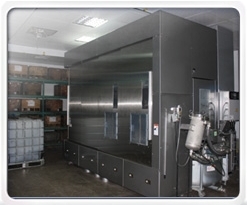
Reduce metal/particle level to meet customer request
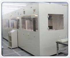
Scan wafer surface by automatioc machine to ensure the particle and defect under certain level
To prevent fraud from impersonating the staff of GlobalWafers Co., Ltd. (“GWC”), of any financial institutions, or other identities in order to commit fraud, GWC hereby reminds you that our staff will never ask you to use an ATM, remit money, provide personal information, and/or make calls to / call back any suspicious number. GWC’s staff will not ask financial institutions to give you the above instructions on our behalf.
Because the caller ID can be faked, if you receive any call that the caller ID is GWC or its number starts with “+”, “+03” or “+886”, or the caller’s statement, instruction or accent is weird, please hang it up and directly contact our staff(Human Resources Department / Mr. Chen 03-5791213), and we also encourage you to call 165 anti-fraud hotline in order to protect your lawful rights.