

In response to the global trend toward high performance and low carbon emissions, GlobalWafers continues to advance smart manufacturing by leveraging technological innovation to drive process upgrades and energy management efficiency. Recently, the company introduced artificial intelligence (AI) image recognition technology into the wafer crystal growth process. This enables precise control of melting and feeding timing, further improving operational efficiency, process stability, and energy utilization. The technology not only enhances productivity and yield through digitalization, but also reduces energy consumption and carbon emissions, demonstrating the dual benefits of digital transformation and green transition. It serves as a concrete example of how smart manufacturing and sustainable development can move forward hand in hand.
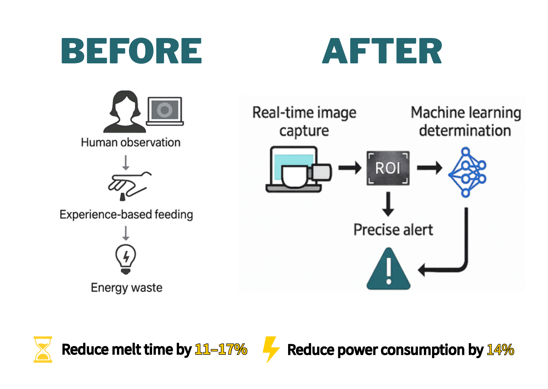
One of the challenges in the crystal growth process lies in determining the optimal timing for material replenishment. If replenishment occurs too early or too late, it can result in energy waste. In the past, due to reliance on subjective experience, it was difficult to consistently monitor the actual progress of silicon melting and consumption, requiring prolonged periods of high-power heating and thus reducing energy efficiency. As process requirements continue to rise, GlobalWafers has been actively introducing AI technology, shifting from the traditional model of relying on human judgment to a technology-driven approach based on “objective image data” to achieve smart manufacturing.
The AI image recognition system deployed by GlobalWafers can learn complex and nonlinear characteristics such as melt surface patterns, contrasts, and hierarchical changes, thereby enhancing its ability to identify different melt conditions. By incorporating differential techniques and adaptive filter designs, the system effectively strengthens noise resistance, enabling it to perform reliably even under limited image quality or fluctuating lighting conditions.
The AI system can detect grayscale variations at different melt stages in real time and automatically issue feeding signals at the appropriate moments. Compared with traditional manual judgment, the system can complete analyses within seconds. Through rapid automated detection and feedback, it significantly improves both the accuracy and efficiency of feeding decisions while avoiding additional compensatory heating.
The benefits of this technology are clear, delivering both process optimization and energy-saving outcomes while embodying the value of digital and sustainability-driven “dual transformation”:
- Improved Efficiency: Overall melting time is reduced by approximately 11-17%, helping to enhance production line utilization and operational performance.
- Reduced Energy Consumption: Each crystal puller can save an average of about 14% in electricity consumption, effectively reducing energy loss and carbon emissions caused by additional heating.
- Optimized Human Operation: The system alleviates the stress and burden on operators who previously had to monitor the melt surface for extended periods, reducing the risk of human error while improving comfort and consistency.
The adoption of this technology underscores GlobalWafers’ ongoing investment in smart manufacturing and energy management. It also reflects the company’s commitment to implementing energy conservation and carbon reduction through a scientific and data-driven approach. As a successful case combining digitalization and decarbonization, it aligns with the industry’s active pursuit of “dual transformation.” Looking ahead, the company will continue to advance its smart manufacturing blueprint, drive process upgrades and operational optimization, and steadily move toward the goals of high performance, low carbon, and sustainable development.