
Group Profile
Company Profile
The predecessor of GlobalWafers was the Semiconductor Business of SAS (Sino-American Silicon Products Inc), founded in Hsinchu Science and Industrial Park, 1981. Subsequently, SAS focus on the solar energy field with production lines for solar cells and modules. SAS also engages in downstream power generation system businesses to become one of the most comprehensive vertical-integrated companies nationwide. SAS has actively adjusted its product sales strategy and expanded into silicon material application products in order to expand the product application fields.
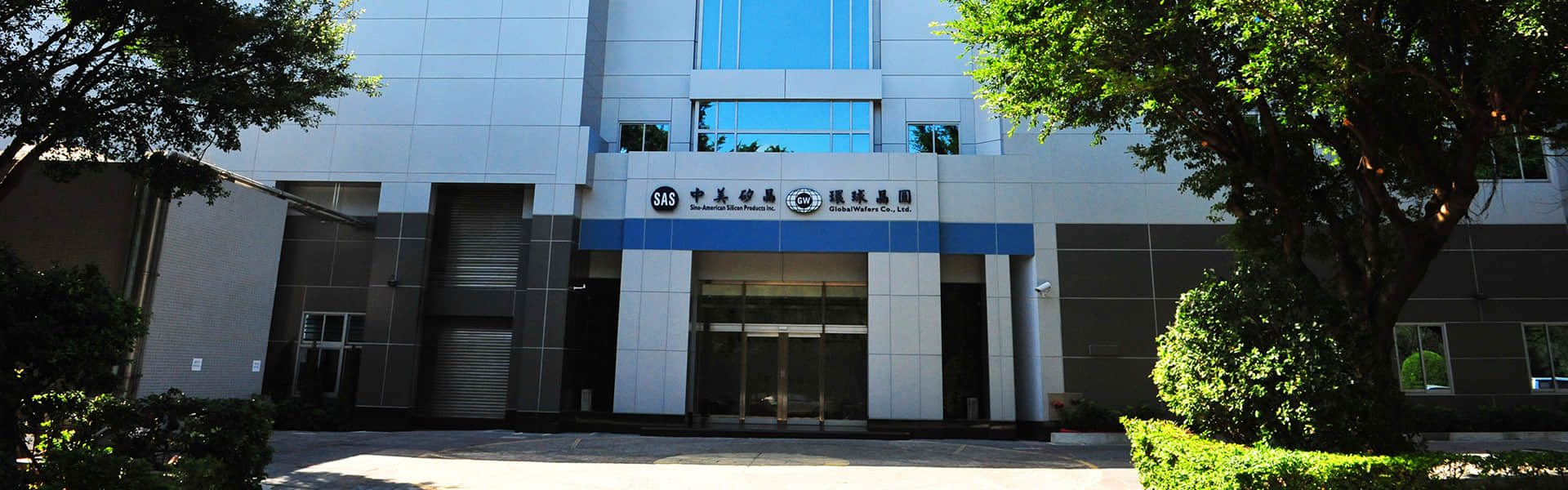
GlobalWafers Co., Ltd. is Taiwan’s largest, world’s third-largest and largest non-Japanese wafer manufacturer that specializes in 3” to 12” silicon wafer manufacturing, possessing complete production lines from ingot growth, slicing, etching, diffusion, polishing and epitaxy. Its high value products include Epi wafers, polished wafers, diffusion wafers, annealed wafers, SOI wafers, FZ wafers and compound wafers. Whether in terms of expertise consulting, mutual development or after service, GlobalWafers has received praise from both domestic and foreign customers. Product applications extend through power management, automotive, IT and MEMS.
GlobalWafers shall devote itself to semiconductor products expansion, quality improvement and customer satisfaction. GlobalWafers aims to become the best wafer supplier and provide total solution and maintain positive growth of the company together with our customers and partners by offering them the best quality, technology and service, and creates greater values to our customers, shareholders and employees.
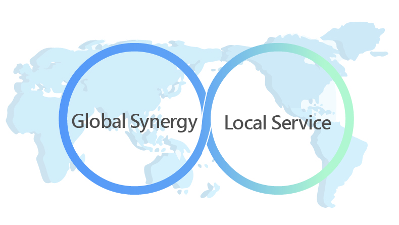
Global Synergy
Local Service
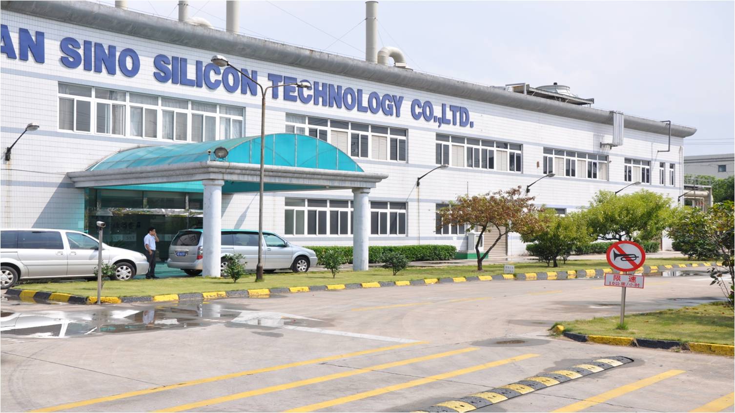
Deployment in Mainland China – SST
To globalize products and realize the idea of international industry cooperation -“Global Synergy, Local Service” – SAS, the parent company of GlobalWafers, established SST in Mainland China, in 1999 to provide 4”~8” wafers to increase the production flexibility, exploring potential market, and serving local customers. After the formal carve-out on October 1, 2011, SST has become GlobalWafers’ subsidiary with 100% shareholding. .
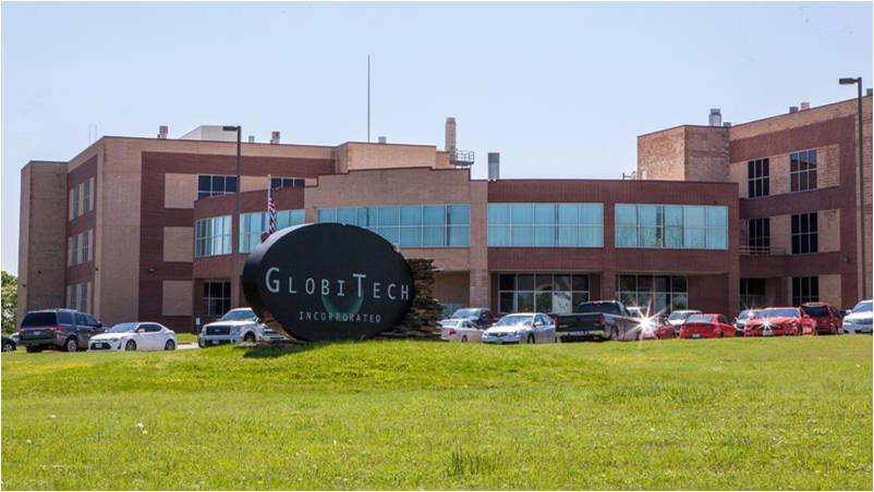
Deployment in USA
GlobiTech
SAS, the parent company of GlobalWafers, acquired American company GlobiTech as a 100% shareholder on April 1, 2008. After the formal carve-out on October 1, 2011, GlobiTech has become GlobalWafers’ subsidiary with 100% shareholding. The acquisition has combined GlobiTech’s epitaxial expertise and customer value with GlolbalWafers’ superior management experience, equipping GlolbalWafers with process capability from ingot growing, to slicing, grinding, polishing and epitaxial deposition; it also helps GlobalWafers entering into high-value 6” and 8” epitaxial wafering business. Via the acquisition, GlobalWafers not only acquires an excellent technical and management team of silicon and epitaxial wafers, but also builds direct contact to tier-1 companies.
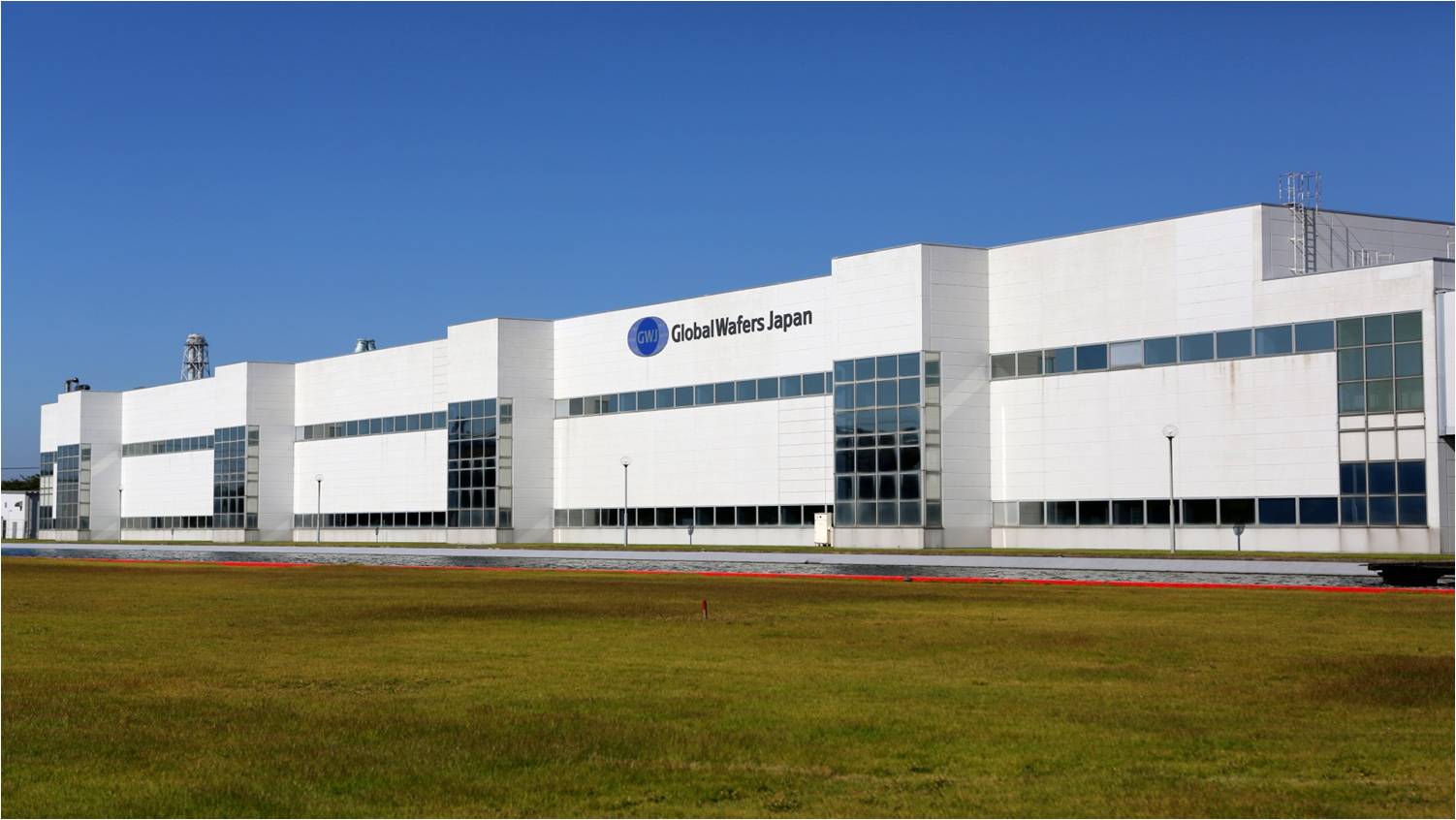
Deployment in Japan
GlobalWafers Japan
To enlarge semiconductor business scale and improve integration and market share, GlobalWafers acquired 100% equity of Covalent Silicon Corporation, the silicon wafer business of Covalent Materials Corporation’s, also the sixth-largest manufacturer in the world. On January 1, 2013, Covalent Silicon Corporation was renamed GlobalWafers Japan. Besides superior core technology, capacity expansion and tier-1 customers, the acquisition also increases operation synthesis and value as well as completes the product portfolio, including 3”, 4”, 5”, 6”, 8” and 12” wafers. GlobalWafers is no doubt the professional supplier of all wafer series.
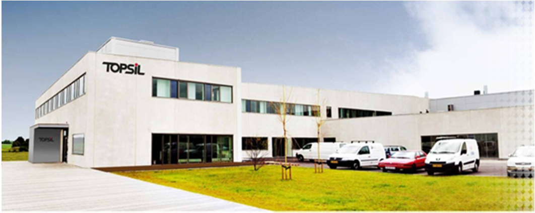
Deployment in Europe
Topsil Semiconductor Materials A/S
In the consideration of global strategy and efficient utilizations of resources, GlobalWafers acquired the silicon activities of Topsil in July, 2016. Topsil Semiconductor Materials A/S (“Topsil”) headquartered at Copenhagen in Denmark, is a leading pioneer of neutron transmutation doped (NTD) float zone (FZ) silicon wafers. Topsil’s 3”–8” FZ wafers were widely recognized in automobile and high power applications because of its superior technology and quality. The acquisition not only helped GlobalWafers successfully step into the FZ wafers, but also added two more modern European plants to global deployment, further strengthening GlobalWafers’ operation scale with enhanced sales channels to expand the market in Europe. The high efficiency product line will also make the portfolio more complete to meet the demand of automobile and high power applications for GlobalWafers, strengthening it future position in the global semiconductor market.
Global Deployment
SunEdison Semiconductor
GlobalWafers successfully acquired SunEdison Semiconductor on 2016/12/2. The combined entity brought together GlobalWafers’ unparalleled operating model and market strengths with SunEdison Semiconductor’s expansive global footprint and product development capabilities. GlobalWafers will see a meaningful expansion of its production capabilities and breadth in product and global customer base, including greater access to the Korea and EU as well as SOI product technologies and capacity. It will also have a significant increase in financial scale. GWC had completed all diameters wafer manufacturing from 3” to 12”, all types of wafers including epi-wafers, annealed wafers, polished wafers, diffusion wafers, leading high-tech SOI and FZ wafers. Moreover, GWC is possessing 18 sites over the world located in 9 countries including Taiwan, China, USA, Japan, Demark, Korea, Italy, Malaysia and Singapore to provide worldwide customers the most efficient, effective and highest quality services as well as superior strategic position in supplier risk management for all customers.
Strategic Alliance / Maximizing Synergy
GlobalWafers enhances its operation performance via integration through strategic alliance and reinvestment in USA, China and Japan. We aggressively yet steadily expand business spectrum and market share in the principle of maximizing shareholder profit. GlobalWafers aims at become the leader in global wafering.
- Full Company Name : GlobalWafers Co., Ltd.
- Founded Date : 2011/10/18
- Paid-in Capital : NT$ 4,781.14 Million
- Products and Services : Research, develop and design on semiconductor ingots/wafers
- Chairperson : Doris Hsu
- President : Mark England
- Tel : +886-3-577-2255
- Fax : +886-3-578-1706 / +886-3-579-0405
- Address : No. 8, Industry E. Rd. II, Hsinchu Science Park, Hsinchu City, Taiwan