
GlobalWafers Global Expansion Plan
GlobalWafers’ global expansion plan is progressing steadily, with its operations across the Americas, Europe, and Asia becoming increasingly interconnected and mutually supportive, forming a flexible and resilient global manufacturing network. This strategic layout aligns with the semiconductor industry’s long-term trend toward GLOCAL operations — global coordination with localized manufacturing — while strengthening the company’s ability to withstand market fluctuations and geopolitical risks.
Overview of Expansion Projects
Through these expansions, GlobalWafers is establishing end-to-end advanced wafer manufacturing capabilities — from crystal growth to epitaxy — across all three continents. This comprehensive footprint not only supports regional production for global customers but also strengthens the company’s operational resilience and long-term competitiveness.
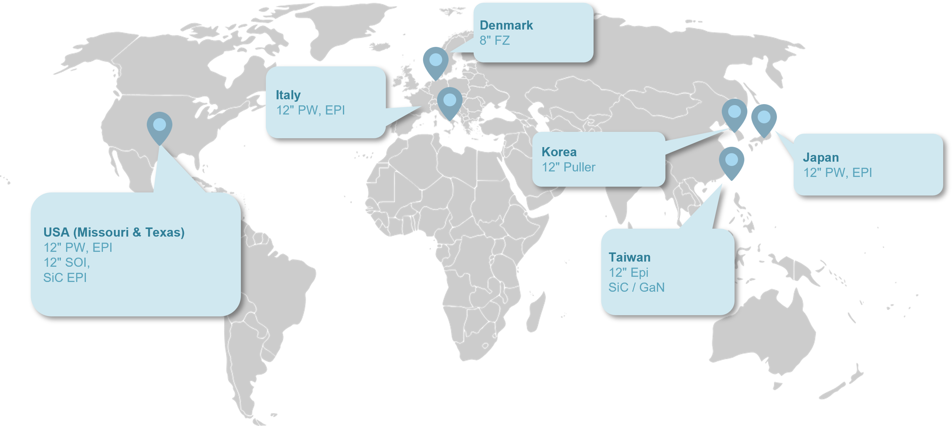
- GlobalWafers America, GWA (Texas, USA)
Located in Texas, GlobalWafers America (GWA) serves as GlobalWafers’ flagship site in North America. The facility focuses on 12-inch polished and epitaxial wafers used in logic, memory, and high-performance computing (HPC) applications—making it a strategically significant advanced wafer manufacturing base within the U.S. semiconductor supply chain. GWA is the first newly constructed 12-inch silicon wafer fab in the U.S. in over two decades, featuring fully integrated capabilities from crystal growth to epitaxy. It enables local support for U.S. semiconductor manufacturers while shortening supply lead times. Officially inaugurated in May 2025, the fab has entered customer sampling and qualification, progressing steadily toward mass production.
GWA has been designated by the U.S. government under the CHIPS and Science Act’s Advanced Manufacturing Support Program, becoming one of the first semiconductor materials projects to receive support. According to the U.S. Department of Commerce and the National Institute of Standards and Technology (NIST), GlobalWafers’ investments in Texas and Missouri are eligible for up to USD 406 million in CHIPS Act funding, disbursed in stages based on construction and production milestones. This support represents a major milestone in strengthening the U.S. wafer supply chain, as GWA will help close the long-standing gap in domestic 300 mm wafer supply and advance a more self-sufficient U.S. semiconductor ecosystem.
In addition, under the Advanced Manufacturing Investment Credit (AMIC) program, investments made after 2026 will be eligible for a 35% investment tax credit (up from 25%), further enhancing long-term competitiveness. The USD 3.5 billion project has already created over 1,200 construction-related jobs and 180 permanent positions in northern Texas, and is expected to hire up to 650 engineers, technicians, and operations professionals by 2028.
GlobalWafers upholds ESG as a core mission, with all subsidiaries committed to green manufacturing. Once GWA enters mass production, it will produce the world’s most advanced silicon wafers using 100% renewable energy, achieving the company’s goal of sustainable manufacturing. GlobalWafers remains dedicated to advancing next-generation semiconductor innovation while minimizing environmental impact, demonstrating that technological progress and sustainability can move forward together.
- MEMC LLC (Missouri, USA)
Located in St. Peters, Missouri, MEMC LLC is one of GlobalWafers’ key technology and manufacturing bases in the United States, specializing in 12-inch Silicon-on-Insulator (SOI). It is the only 12-inch SOI wafer manufacturing facility in the U.S., playing a critical role in high-performance computing (HPC), automotive electronics, communications, and sensor applications—supporting the localization of advanced process technologies in the United States. The site has entered sampling and customer qualification, with stable operational progress.
Like the Texas fab, MEMC is part of the CHIPS and Science Act’s Advanced Manufacturing Support Program, representing one of the two cornerstone investments reinforcing the U.S. wafer supply chain. According to announcements from the U.S. Department of Commerce and NIST, GlobalWafers’ Texas and Missouri investments together qualify for up to USD 406 million in CHIPS Act funding, to be disbursed progressively as project milestones are achieved. MEMC is also eligible for the Advanced Manufacturing Investment Credit (AMIC), allowing a 35% investment tax credit (raised from 25%) starting in 2026, further strengthening its long-term competitiveness.
Throughout its construction and ramp-up, MEMC has continued to expand local employment, collaborate with U.S. universities and research institutions, and advance semiconductor materials R&D and talent development, contributing to the creation of a more complete U.S. advanced materials and manufacturing ecosystem.
Aligned with GlobalWafers’ core value of green manufacturing, the new production line will operate with 100% renewable energy once in full mass production, minimizing process energy consumption and carbon footprint while maintaining world-class product quality—demonstrating the company’s long-term commitment to innovation and sustainable transformation.
- MEMC Electronic Materiels S.p.A. / FAB300 (Novara, Italy)
Located in northern Italy, FAB300 in Novara serves as GlobalWafers’ flagship 12-inch wafer manufacturing base in Europe and is among the few facilities in the region with fully integrated process capabilities. Its main products include 12-inch polished and epitaxial wafers for logic, memory, power devices, and sensors—supporting Europe’s goals for semiconductor autonomy and the energy transition.
FAB300 was officially inaugurated in October 2025, has begun pilot shipments, and is currently in customer qualification and volume ramp-up. The total investment amounts to €450 million, supported by the European Union’s Important Project of Common European Interest (IPCEI) – Microelectronics and Communication Technologies, with subsidies totaling €103 million (around 25% of total investment), disbursed progressively with construction and production milestones.
FAB300 strengthens Europe’s semiconductor supply chain localization and contributes to the region’s RE100 sustainability goals. Once reaching full production, the fab will operate with 100% renewable energy and target 50% water recycling efficiency, while creating approximately 150 technical and engineering jobs, fostering regional high-tech industry growth.
Through close collaboration with European customers and governments, GlobalWafers continues to promote sustainability and technological innovation in tandem, ensuring FAB300 serves as a critical hub connecting its operations in Asia and the Americas—enhancing the group’s global resilience and technological leadership.