
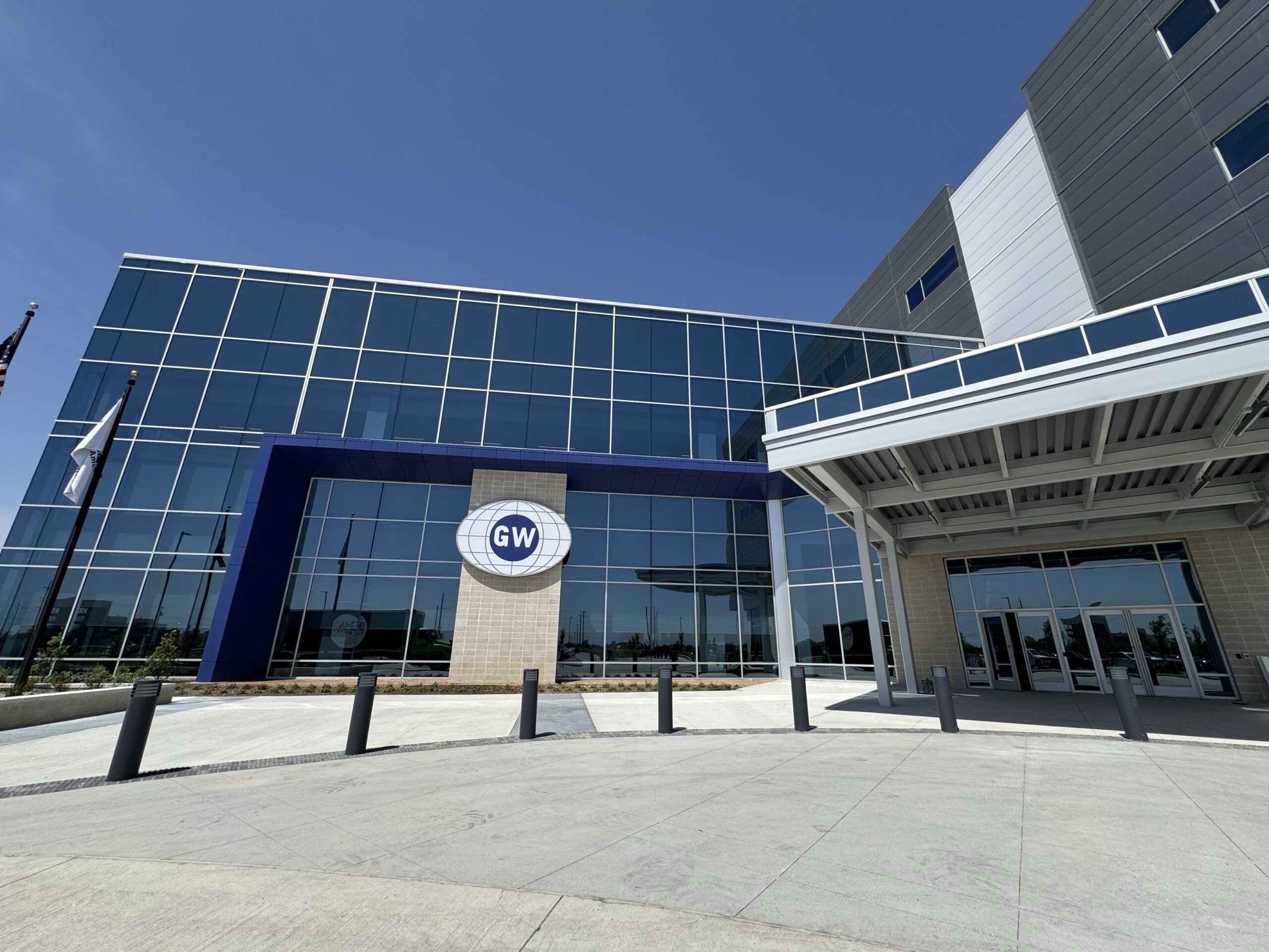
GlobalWafers America, the industry’s most advanced fully integrated 300mm semiconductor wafer facility, officially opens for business.
GlobalWafers Co., Ltd. Chairperson Doris Hsu officially opens GlobalWafers America, the industry’s most advanced fully integrated 300mm semiconductor wafer facility and announces the company’s intention to further expand the GWA operation in alignment with market growth and Trump Administration priorities.
SHERMAN, Texas and HSINCHU, Taiwan, May 16, 2025 – On May 15 (U.S. time), GlobalWafers Co., Ltd. (GWC, 6488:TT) hosted U.S. Investment Accelerator Executive Director Michael Grimes, Taiwan Minister of Economic Affairs Kuo Jyh-huei, AIT Director Raymond Greene, ROC Taiwan’s Representative to the United States Alexander Yui, Sherman Mayor Shawn Teamann, and hundreds of customers, suppliers, and partners in Sherman, Texas to celebrate the Grand Opening of GlobalWafers America (GWA), the company’s newest and most advanced 300mm silicon wafer manufacturing facility.
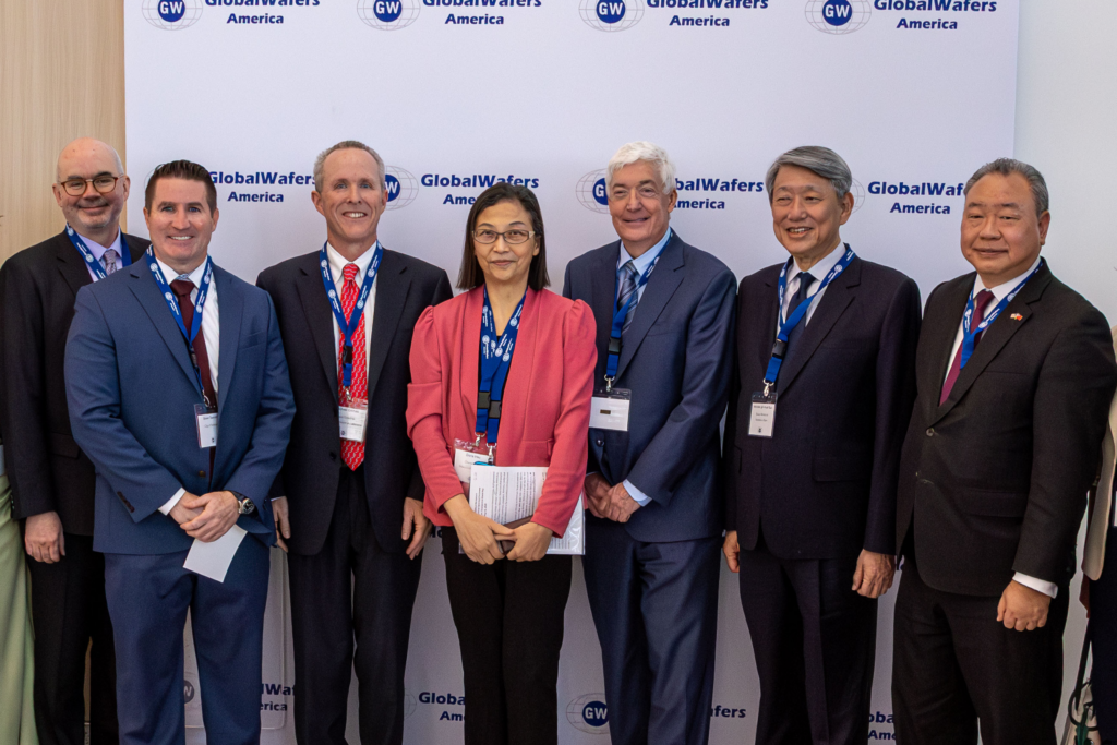
GlobalWafers celebrated the Grand Opening of GlobalWafers America in Texas with honorable guests from Taiwan and the United States. (From left to right) AIT Director Raymond Greene, Sherman Mayor Shawn Teamann, U.S. Investment Accelerator Executive Director Michael Grimes, GlobalWafers Chairperson Doris Hsu, GlobalWafers President Mark England, Taiwan Minister of Economic Affairs Kuo Jyh-huei, and ROC Taiwan’s Representative to the United States Alexander Yui.
GlobalWafers made the decision to build its flagship facility in the United States in May 2022 and held the groundbreaking ceremony in Sherman on December 2, 2022. To date, the US$3.5 billion project has created 1200 construction and 180 permanent jobs in North Texas and will employ up to 650 engineering, technical and operational professionals by the end of 2028.
During the celebration Chairperson Doris Hsu unexpectedly announced the company’s plan to further grow its U.S. manufacturing base, stating: “On the three-year anniversary of our decision to build GWA, I am pleased to announce GlobalWafers’ intention to expand our current U.S. investment by another $4 billion to reach $7.5 billion!” In alignment with growth in market demand- combined with an advantageous tariff structure favoring cost effective U.S. expansion- GlobalWafers expects to add phases 3 and 4 to its existing commitment in Sherman. As the only advanced wafer supplier manufacturing in the United States, this additional investment, bolstered by ongoing support from the U.S. Government and the Trump Administration, is expected to fully secure the advanced wafer supply needed to power a broad range of next-generation technologies and innovation.
![]()
GlobalWafers Chairperson Doris Hsu officially opens GlobalWafers America
On this point, GWC President Mark England noted: “GWA will fill a key vulnerability in the U.S. supply chain and help build a more complete and self-sufficient local semiconductor ecosystem — one that is more resilient and future-ready.” In fact, GWA is the only fully integrated advanced silicon wafer manufacturing facility participating in the U.S. Government’s CHIPS for America Program and is the first production line of its kind built in the United States in over 20 years.
Under the CHIPS Program- now part of President Trump’s new U.S. Investment Accelerator- the U.S. Department of Commerce is investing US$406 million in GlobalWafers’ new U.S. operations in a strategy to rebuild a key node of the U.S. semiconductor supply chain. At the event, U.S. Investment Accelerator Executive Director Michael Grimes observed: “GlobalWafers investment is a great example of the return of United States manufacturing in a critical industry. President Trump and Secretary Lutnick have made it a fundamental objective to bring semiconductor manufacturing home to America. Through our work with GWA, we are ensuring that the essential starting material for advanced chips is manufactured right here in United States. GlobalWafers current investment, together with its new commitment announced today, will secure U.S. wafer supply for generations to come.”
The City of Sherman, Grayson County, and the State of Texas have also provided important incentives in the form of land, direct grants, tax incentives and excellent manufacturing infrastructure. Chairperson Doris Hsu noted, “There is simply not a more welcoming location in all the United States for doing business than Texas, Grayson County and Sherman. They have worked strategically to build the Silicon Prairie and GWA is thrilled to be part of it.” Governor Greg Abbott remarked, “We are proud that GlobalWafers America is now calling Texas home. GWA is rounding out the already well-established Texas semiconductor ecosystem, setting Texas apart as the only state in the country with advanced silicon wafers.”
From construction to production, GlobalWafers has partnered with hundreds of best-in-class suppliers who have also brought advanced engineering systems, technology and business processes to the project. “Without construction partners, toolmakers and materials suppliers also pushing the edge of their capabilities, GWA would not be able to deliver the quality wafers our customers have come to expect from GlobalWafers,” said GWA VP of Operations Wyatt Watson. “The GWA project has brought out the best of our entire supply chain.”
GlobalWafers is one of five global suppliers of advanced semiconductor wafers and the only one expanding in the United States during this new era of supply chain regionalization. Along these lines, Ashlie Wallace, GlobalFoundries’ SVP of Global Supply Chain, echoed the sentiment of many customers noting, “As a longstanding strategic partner, we are pleased to see GlobalWafers increasing domestic supply of silicon wafers critical to the essential semiconductors we manufacture.”
300mm silicon wafers are the essential input used by foundries and integrated device manufacturers to produce leading-edge, mature-node, and memory chips. Silicon from GWC’s semiconductor wafers is found in essentially every device that powers modern life– from home appliances, automobiles and physical infrastructure to cell phones, computers, and AI applications.
Further to the strategic phase 3 & 4 expansion announced today, GWA’s new 142-acre campus in Sherman— designed to accommodate up to six phases — has space to add two additional phases and significantly grow capacity in lockstep with chip producers who have collectively announced over US$500 billion in new U.S. investments over the next decade.
As part of our core ESG commitment, GlobalWafers companies worldwide practice green manufacturing. Once fully ramped, GWA will run on 100% renewable energy to produce the world’s most advanced silicon wafers. Across the GlobalWafers family, we remain deeply committed to minimizing our environmental impact while enabling the next generation of semiconductor innovation.
GlobalWafers Co., Ltd., the world’s third largest supplier of semiconductor wafers, maintains 18 manufacturing and operational sites spanning three continents and nine countries. The company is one of the global leaders in semiconductor technology, providing innovative and advanced technology solutions to leading chip manufacturers to transform lives around the world.